

Key Environmental Tests for Semiconductors
Semiconductors are highly sensitive to environmental conditions such as temperature, humidity, voltage stress, and mechanical strain. Environmental tests simulate real-world conditions that devices might encounter during their lifecycle, allowing manufacturers to identify potential failure points before products hit the market.
The increasing complexity of semiconductor devices—especially with innovations like chiplet technology—demands rigorous testing standards to mitigate risks like Electrochemical Migration (ECM), thermal degradation, and mechanical failures.
ESPEC’s comprehensive range of testing equipment, available in the UK and Ireland from Unitemp positions it as a key partner for UK semiconductor manufacturers aiming to deliver high-quality, reliable products.
Key Environmental Tests and ESPEC’s Advanced Solutions
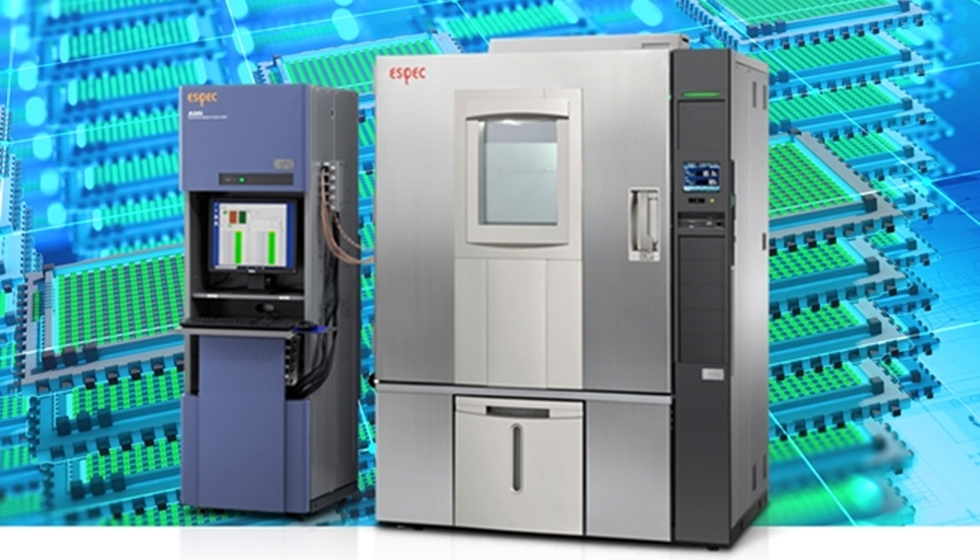
Temperature and Humidity Testing
Purpose: Assess how semiconductor devices perform under varying temperature and humidity levels, identifying potential issues like corrosion, insulation failure, or material degradation.
ESPEC Solutions:
- Temperature (& Humidity) Chambers: ESPEC offers a range of chambers capable of precise temperature and humidity control, allowing for accurate simulation of environmental conditions.
- Platinous Series: These chambers provide a wide temperature and humidity range, ensuring comprehensive testing capabilities for various semiconductor applications.
Electrochemical Migration (ECM) Testing
Purpose: Evaluate the risk of ECM, where metal ions migrate under electric fields and humidity, potentially causing short circuits in miniaturized circuits.
ESPEC Solutions:
- Electro-Chemical Migration Evaluation System (AMI): This system measures insulation resistance with high precision, detecting early-stage ECM and ensuring the reliability of high-density semiconductor designs.
High Voltage Bias Insulation Resistance Testing
Purpose: Determine the insulation resistance of semiconductor components under high voltage conditions to ensure they can withstand operational stresses without breakdown.
ESPEC Solutions:
- High Voltage Bias Insulation Resistance Evaluation System: This system applies high voltage to components while measuring insulation resistance, identifying potential weaknesses in the dielectric materials.
High Temperature Reverse Bias (HTRB) Testing
Purpose: Assess the reliability of semiconductor devices under high temperature and reverse bias conditions, which can reveal potential failure mechanisms.
ESPEC Solutions:
- HTRB Test System: ESPEC’s system subjects devices to elevated temperatures and reverse bias voltages, accelerating stress conditions to identify latent defects.
Electromigration Evaluation
Purpose: Investigate the movement of metal atoms in interconnects under high current densities, which can lead to open circuits over time.
ESPEC Solutions:
- Electromigration Evaluation System (AEM Series): This system applies controlled current to test structures, monitoring resistance changes to evaluate electromigration effects.
Time-Dependent Dielectric Breakdown (TDDB) Testing
Purpose: Evaluate the longevity and reliability of dielectric materials under continuous electrical stress, predicting the time to failure.
ESPEC Solutions:
- TDDB Evaluation System: ESPEC’s system applies constant voltage stress to dielectric layers, monitoring leakage currents to assess breakdown characteristics over time.
Temperature Humidity Bias (THB) Testing
Purpose: Determine the resistance of semiconductor devices to combined temperature, humidity, and electrical bias conditions, which can accelerate corrosion and other failure mechanisms.
ESPEC Solutions:
- THB Evaluation System: This system subjects devices to controlled temperature, humidity, and bias conditions, monitoring performance to identify potential reliability issues.
For more information on ESPEC’s semiconductor testing solutions, visit our semiconductor testing and measurement & evaluation systems page.
For more information on Key Environmental Tests for Semiconductors talk to Unitemp Ltd