

The increasing complexity of semiconductor devices, driven by advancements in chiplet technology, 3D integration, and ultra-miniaturisation, has made reliability testing more critical than ever. As circuit densities increase, so does the risk of failure mechanisms such as Electrochemical Migration (ECM) and insulation breakdown under electrical stress. The ESPEC AMI System is designed specifically for high-precision evaluation of these failure modes. It provides engineers with the ability to assess insulation degradation under electrical, thermal, and humidity stress conditions—key factors in ensuring semiconductor device reliability across various applications.
Technical Capabilities of the ESPEC AMI System
- High-Accuracy Insulation Resistance Measurement
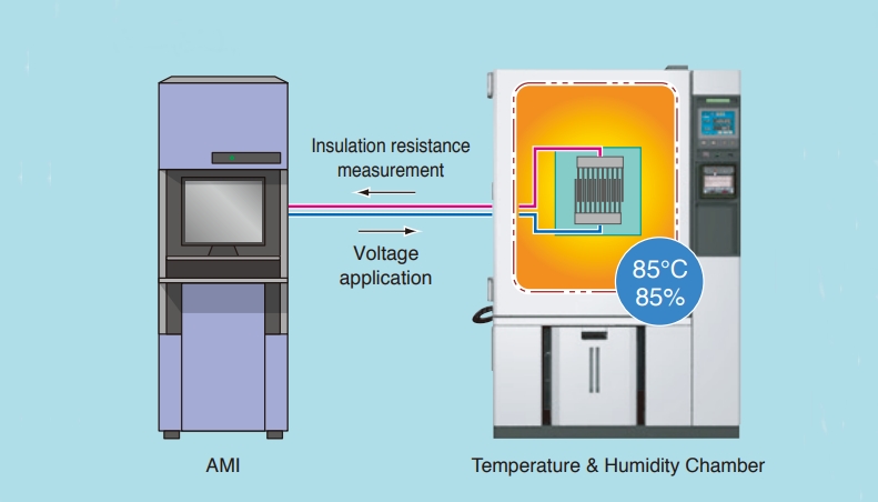
The core of the AMI system is a high-sensitivity electrometer, which delivers precise insulation resistance measurements. This allows for early detection of electrical leakage paths and insulation failures that can compromise semiconductor performance, particularly in high-density packaging environments.
- Multi-Channel Measurement
The system supports up to 150 independent channels per electrometer, allowing parallel testing of multiple devices or nodes within a circuit. This capability is essential for high-throughput environments, such as wafer-level or packaged device reliability screening.
- Environmental Stress Integration
The AMI system is designed for use with ESPEC’s temperature and humidity chambers, including the AR Series and Platinous Series. This allows for simultaneous testing under controlled environmental conditions, replicating real-world operational stresses like temperature cycling, high humidity, and combined temperature-humidity bias testing (THB).
- Electrochemical Migration (ECM) Evaluation
With increasingly fine circuit geometries, ECM has become a critical failure mechanism in modern semiconductor devices. The AMI system performs evaluations under specific voltage and environmental stress conditions to detect potential pathways for metal ion migration. Key parameters measured include:
- Stress Voltage: Applied to replicate real-world electrical stress conditions.
- Measurement Voltage: Monitors for any drop in insulation resistance indicative of ECM onset.
- Automated Test Sequencing
The system incorporates advanced scanner and relay units, allowing automated switching across channels. This reduces human error, increases throughput, and ensures consistency during extended testing cycles.
Applications in Semiconductor Reliability Testing
The ESPEC AMI system is suitable for a range of semiconductor reliability assessments, including:
- Chiplet and Advanced Packaging Evaluation: As chiplet-based architectures become more common, precise testing of interconnect reliability under thermal and electrical stress is essential.
- Substrate and Dielectric Material Testing: Evaluation of substrates, insulating resins, and packaging materials for long-term reliability under high humidity and voltage stress.
- Automotive and Aerospace Electronics: Ensuring that semiconductors meet the stringent reliability requirements necessary for mission-critical applications.
- Telecommunications and IoT Devices: Validation of device longevity under varied environmental and electrical conditions typical of field deployments.
The AMI system evaluates semiconductor components under differing conditions to assess their vulnerability to ECM-related failures. This allows manufacturers to adjust material selection, circuit layout, or protective coatings to mitigate long-term reliability risks. For semiconductor manufacturers focused on ensuring long-term device reliability, the AMI system offers the precision, scalability, and environmental integration needed to meet the highest industry standards. Learn more about the technical specifications and capabilities of the AMI system.
For more information on Advanced Semiconductor Reliability Testing with the ESPEC AMI System talk to Unitemp Ltd