Sign In


Clean-Room Laser Direct Imaging For Pcbs
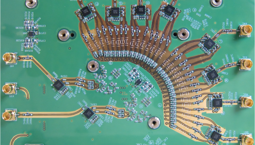
Explore advanced high-tech PCB services including multilayer fabrication up to 60 layers, impedance-controlled designs, RF and mixed-signal layouts, and clean-room laser direct imaging. Benefit from expert PCB simulation using ANSYS HFSS and SIWave, blind and buried via structures, and complete engineering for complex, high-speed electronic applications.
Explore advanced high-tech PCB services including multilayer fabrication up to 60 layers, impedance-controlled designs, RF and mixed-signal layouts, and clean-room laser direct imaging. Benefit from expert PCB simulation using ANSYS HFSS and SIWave, blind and buried via structures, and complete engineering for complex, high-speed electronic applications.
For more information on Clean-Room Laser Direct Imaging For Pcbs talk to Synergie-Cad (UK) Ltd
Welcome back to FindTheNeedle.
Not registered? Get listed — most visitors don't have an account yet.
List your company on FindTheNeedle.