Sign In


New 2D material challenges graphene
11-05-2017
Graphene’s excellent electrical and thermal conductivity make it promising for electronics. The material has garnered a lot of research attention in the short time since its discovery. But the two-dimensional carbon material’s Achilles heel is the lack of a bandgap. Bandgaps, possessed by traditional semiconductor materials like silicon, are required to make the transistors that act as switching elements in logic circuits.
“Huge efforts have been devoted to open the bandgap in graphene by stretching it and/or sandwiching it with other layered materials,” says Jong-Beom Baek, a professor of energy and chemical engineering at Ulsan National Institute of Science and Technology (UNIST). But the processes are cumbersome and difficult to control, he says. So researchers are looking for new 2D materials with tunable electronic properties.
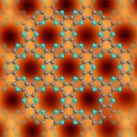
Baek and his colleagues from UNIST and Pohang University of Science and Technology have now developed a new 2D material based on graphene itself by incorporating nitrogen atoms. The new 2D crystal shares the hexagonal lattice structure of graphene, but it is riddled with uniformly distributed holes and nitrogen atoms. Nitrogen atoms replace six carbon atoms around the periphery of each hole, with a C2N stoichiometry in the basal plane. The researchers reported their findings in the journal Nature Communications.
The holey nitrogenated carbon crystal is easy to make using a simple wet chemical reaction. The researchers made a solution of hexaaminobenzene and hexaketocyclohexane, and added a few drops of sulfuric acid. This results in a dark graphite-like solid in the solution that the researchers extracted, cleaned, and freeze-dried. Scanning tunneling microscopy revealed the crystals’ structure.
The reaction of the hexa-amine and hexa-ketone monomers spontaneously generates the holey crystalline 2D network, Baek says. The new 2D crystal has a bandgap of 2.0 eV, which is larger than the 1.11 eV bandgap of silicon. “By localizing the electronic cloud around themselves and holes by creating Mott-type physical resistance, the nitrogen atoms contribute to a band-gap opening in the range of commonly used semiconductor materials,” he says.
The researchers were able to make a solution of the crystals and deposit it on rigid silica and flexible plastic substrates. The deposited films contained multiple stacked layers of the crystals. The team also demonstrated the material’s potential for electronics by using it as the semiconductor layer in a field-effect transistor. The transistors show an on/off ratio of 107, about 100 times higher than that of silicon. The on/off ratio, which correlates to the bandgap, signifies a transistor’s ability to switch current on and off.
The new work is “a major breakthrough in the design and development of 2D materials with new structures and properties,” says Liming Dai, director of the Center of Advanced Science and Engineering for Carbon at Case Western Reserve University. Producing conventional 2D materials like graphene on a large scale is challenging. But the nitrogenated crystals described here can be simply synthesized via a bottom-up wet-chemical reaction. They could be cost-effective to make on a large scale given their scalable solution synthesis method.
For more information on New 2D material challenges graphene talk to Testbourne Ltd
Welcome back to FindTheNeedle.
Not registered? Get listed — most visitors don't have an account yet.
List your company on FindTheNeedle.