

Probe Station – Double-Sided Wafer Probing
What is double-sided wafer probing and why is it needed? (IKB-089)
Most of the wafer probing systems are designed in such a way that the device under test (DUT) is only probe tested from the top side. The manipulators, probe cards, and optical fibres normally contact the sample from above, while the bottom is fixed to a solid chuck and is not accessible for electrical (except for ground or biased connections) or for optical testing. Therefore, the conventional top sided probing configuration, also known as single-sided, is not suitable for testing a large number of photonic, optoelectronic, and MEMS devices, which require double-sided stimulation and/or output detection.
To address these needs, SemiProbe have designed and delivered multiple double-sided wafer probing (DSP) configurations for their probe system for life (PS4L) platforms. The DSP systems have been widely deployed in research and industry in a range of applications, such as standard light emitting diodes (LEDs), edge emitting diodes (EELDs), vertical surface cavity emitting lasers (VSCELs), MEMS, and optical sensors.
Thanks to their unique architecture the DSP systems allow users to:
- Stimulate from the top side and detect the output from the back side
- Stimulate from the back side and detect the output from the top side
- Simultaneously stimulate, detect and probe from both sides
- Detect from the edge
All DSP systems are uniquely designed and the probing accessories are selected to meet customers’ specific needs. Like all PS4L platforms, the DSP systems are modular and upgradable, and can be provided as manual, semi-automatic, or fully automatic versions.
During the operation, the DUT is placed in a customised fixture: they can hold die, partial wafers, or whole wafers depending on the users probing requirements. Top-side and bottom-side platens allow the user to mount manual or programmable manipulators with a variety of probe arms (DC, high frequency, OPTO and more) and probe cards. Similarly, optical fibres, detectors, and integrating spheres can be installed on manual or programmable stages to enable a precise movement of the elements. Upward and downward looking optics and imaging systems are used for accurate placement and alignment of probes, detectors, and fibres on both sides of the device. Additional instruments and optical components, such as mirrors and filters, can be mounted on either side.
If required, temperature control capabilities can be implemented in a DSP system. These are provided by thermal chucks or thermal wands and temperature monitoring instruments. If EMI shielding or light-tight probing environments are needed, a DSP platform can be enclosed in a localised environmental chamber or a dark box.


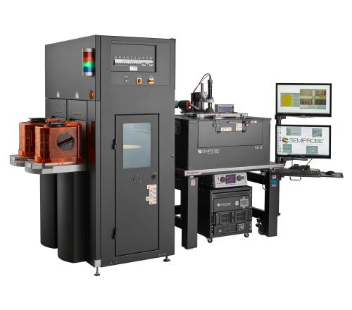
 Example Fully Automatic Double Sided Wafer Probe Station
For more information on Probe Station – Double-Sided Wafer Probing talk to Inseto (UK) Ltd