Sign In


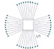
Chip On Board Design is supported within the Pulsonix design environment. With die and bond pad creation available at the 'footprint' level precise pad placement is possible. Die and bond pads are connected to eachother using wires which contain their own rules constraints. In the PCB design editor bond pads can move separately and individually thus creating the optimum pad placement.
For more information on Chip On Board Design talk to Pulsonix
Enquire Now
Welcome back to FindTheNeedle.
Not registered? Get listed — most visitors don't have an account yet.
List your company on FindTheNeedle.